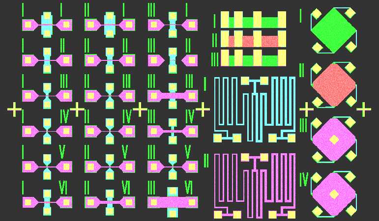
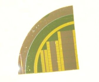
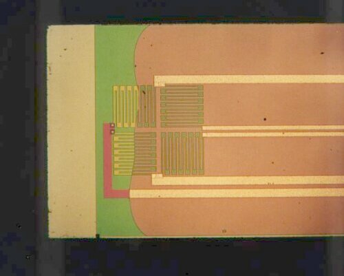
Examples of photomasks design:
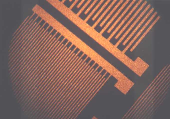
van der Pauw type structures -
left, test of HEMT heterostructures -
middle, contact structures -
right:
|
|
|
|
|
|
|
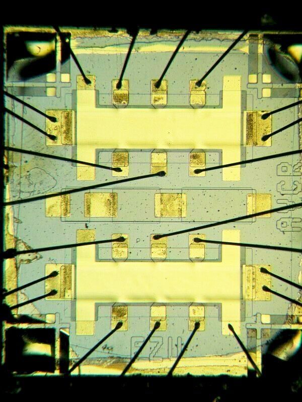
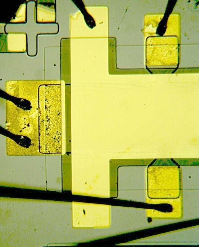
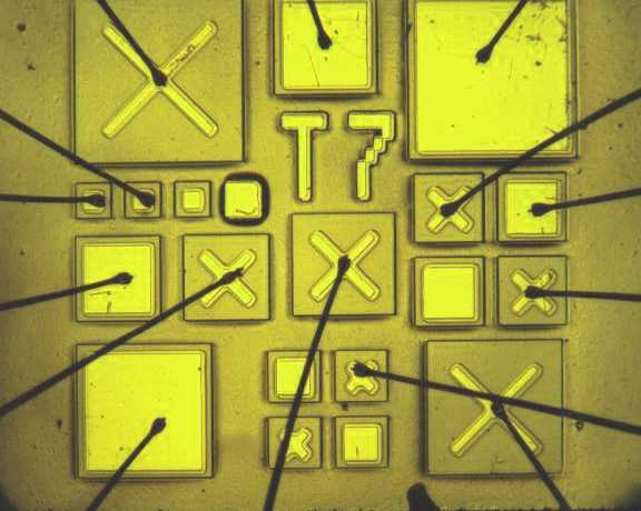
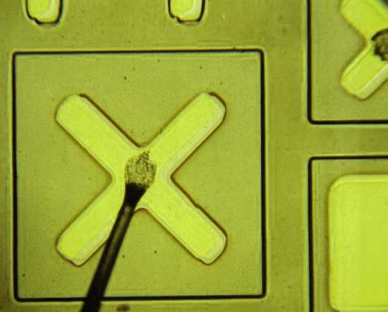
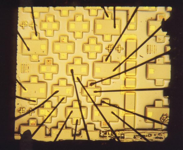
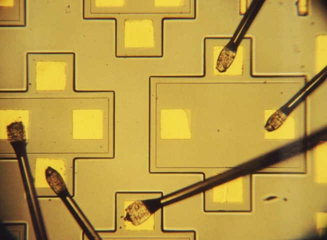
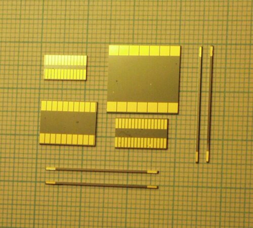
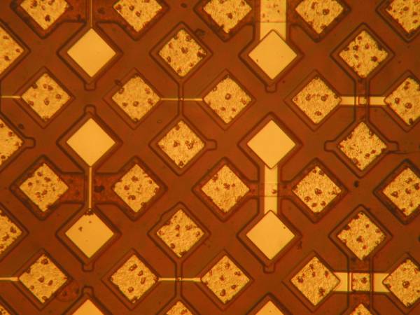 A matrix of resonant-tunnelling diodes (RTDs) and transistors (HEMTs) on the same
heterostructures (square expanded contacts side length = 100 µm ).
A matrix of resonant-tunnelling diodes (RTDs) and transistors (HEMTs) on the same
heterostructures (square expanded contacts side length = 100 µm ).
|
|
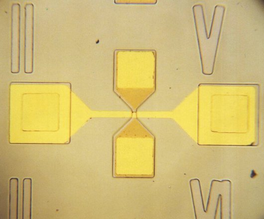
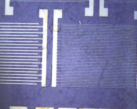
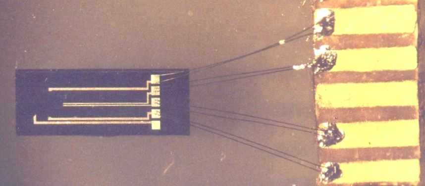
Structures for Hall effect measurements (width of the horizontal gate stripe = 400 µm ) - left,
|
|
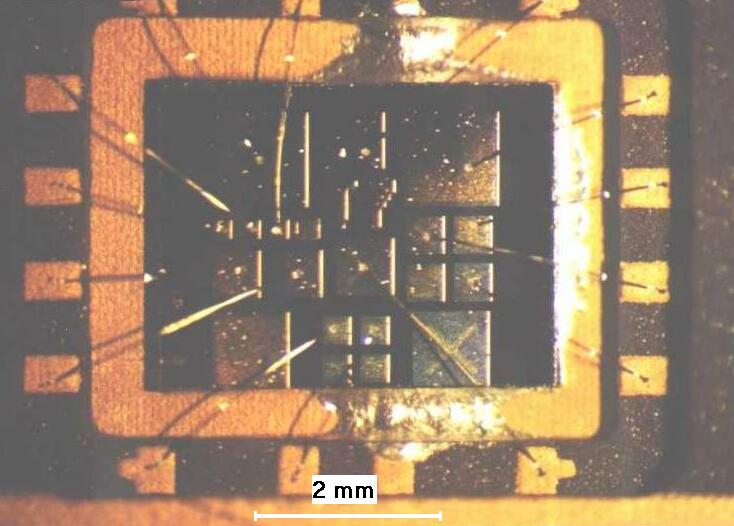
Semiconductor chip comprising a set of photo diodes - left, detail of the central diode - right
|
|
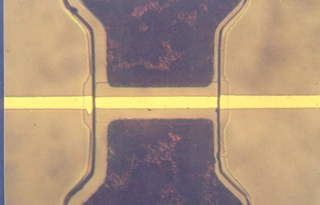
RTD samples prepared on GaAs/GaAlAs heterostructures - left,
|
|
Microstructures based on sputtered piezoresistive layers on silicon substrates:
|
|
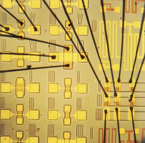
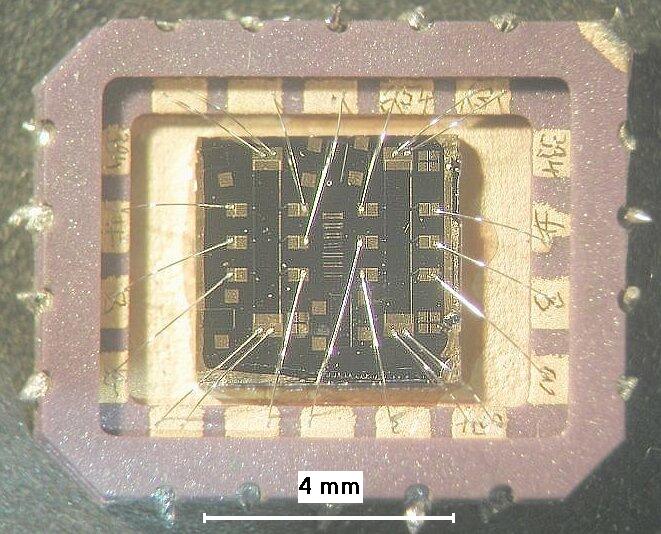
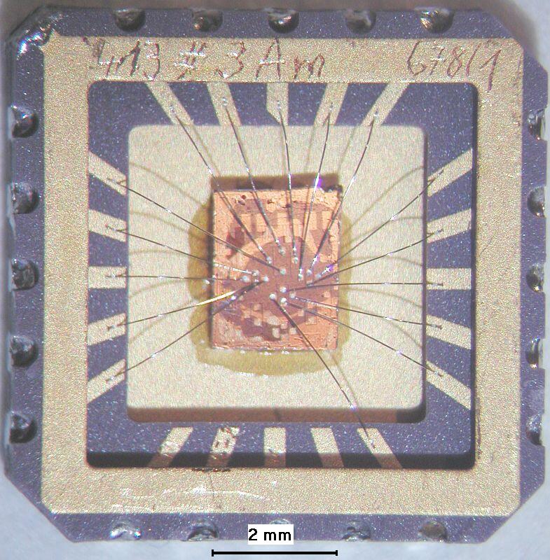
Wired structures in packages designed for their experimental study:
structures for Hall-effect measurements (ceramic chip-carrier package - CCC18) - left,
|
|
|
Floating assembly of a deformation-microsensor silicon chip
- right,
detail of the adjusted microsensor chip structure
- left,
(width of the chip = 2.5 mm ):
|
|
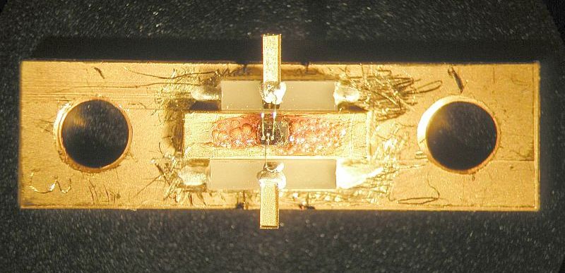
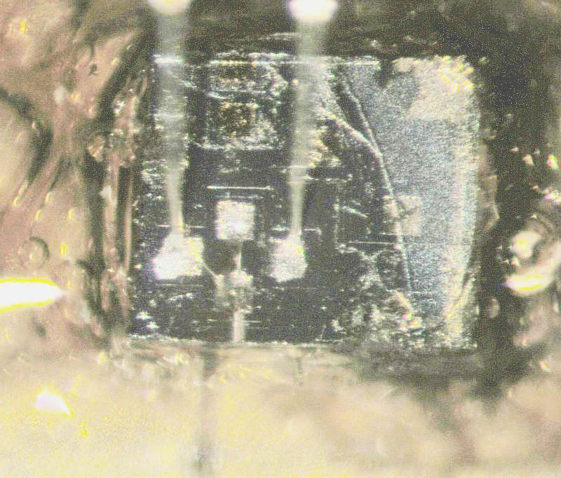
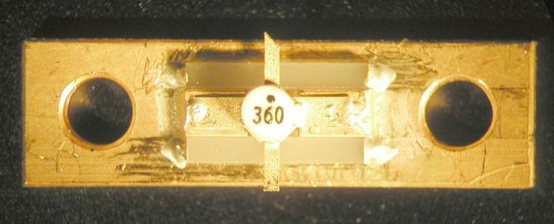
Samples prepared for high-frequency measurements:
RTD assembled - top left,
detail of the bonded RTD chip - right
(expanded contacts side length = 100 µm ),
reference commercial HEMT assembly - 2nd row:
|
|
|
|